Part Number
AD586TQ/883
Analog Devices CDIP Integrated Circuits
Available Stock
40 pcs
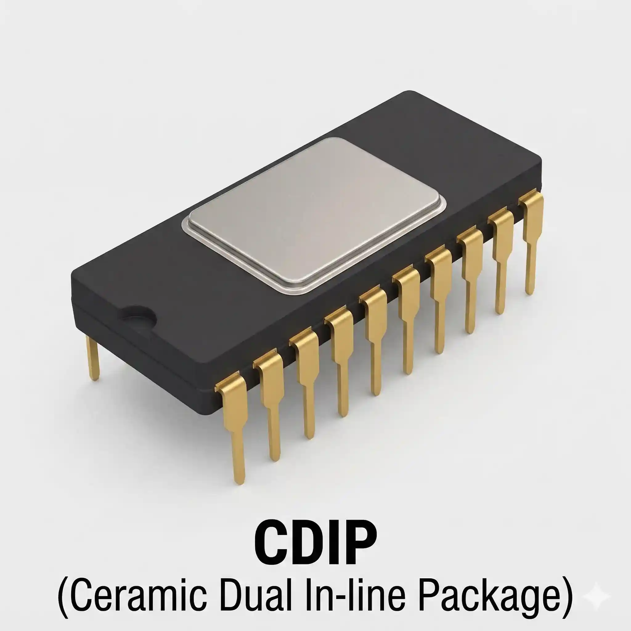
The AD586TQ/883 is a high-precision 5.0 V buried-Zener voltage reference manufactured by Analog Devices in a ceramic dual-inline package (CDIP) and processed to the full MIL-STD-883 Class B screening flow. Devices in this family deliver a laser-trimmed output with tight initial accuracy and a very low temperature drift, typically in the single-digit ppm/°C range across the military temperature spectrum. The buried-Zener architecture provides exceptionally low output noise and excellent long-term stability over thousands of hours, while the hermetic CDIP construction ensures robust performance under shock, vibration, and humidity. Additional features include low line and load regulation, as well as the ability to source and sink up to 10 mA of load current, making the reference suitable as a standalone precision calibration source or as a system benchmark for high-resolution data conversion.
Typical deployments center on mission-critical systems where reliable and accurate DC voltage is essential. These include precision analog-to-digital and digital-to-analog converter references in military avionics, radar signal processing, and satellite telemetry payloads. In the defense sector, the AD586TQ/883 is integrated into weapons guidance, secure communication hardware, and electronic warfare subsystems. Industrial test and measurement equipment, such as automated calibration benches and precision sensor excitation circuits, also benefit from the reference’s drift and noise characteristics. The /883 suffix indicates full compliance with MIL-STD-883 requirements, including thermal cycling, constant acceleration, and burn-in, which significantly reduces field programmability risks and infant mortality. This screening pedigree, combined with Analog Devices’ extended product-life programs for high-reliability references, supports long-term procurement strategies, but design teams should validate the current CAGE code and datasheet revision to confirm active production and export compliance status.
| Attribute | Value |
|---|---|
| Operating Temperature | -55°C ~ 125°C |
| Qualification | MIL-STD-883 |
| Package / Case | CDIP |
| Mounting Type | Through Hole |
| Absolute Maximum Input Voltage (VIN to Ground) | 36 V |
| Absolute Maximum Power Dissipation (25°C) | 500 mW |
| Initial Output Voltage Error | 2.5 mV |
| Output Noise (0.1 Hz to 10 Hz) | 4 µV p-p |
| Output Voltage | 4.9975 V min / 5.0025 V max |
| Output Voltage Drift (Temperature Coefficient) | 10 ppm/°C(−55°C to +125°C) |
| Quiescent Current | 2 mA typ / 3 mA max |
| Short Circuit Current to Ground | 45 mA typ / 60 mA max |
| Lead Temperature (Soldering, 10 sec) | 300°C |
| Specified Performance Temperature Range | -55°C to +125°C |
| Storage Temperature | -65°C to +150°C |
| Base Device | AD586 |
| Load Regulation (Sourcing 0 mA to 10 mA, 25°C) | 150 µV/mA |
| Long-Term Stability | 15 ppm/1000 hr |
Download the current available datasheet for AD586TQ/883.
Download Datasheet