Part Number
SNJ54LVC373AJ
Texas Instruments CDIP Integrated Circuits
Available Stock
210 pcs
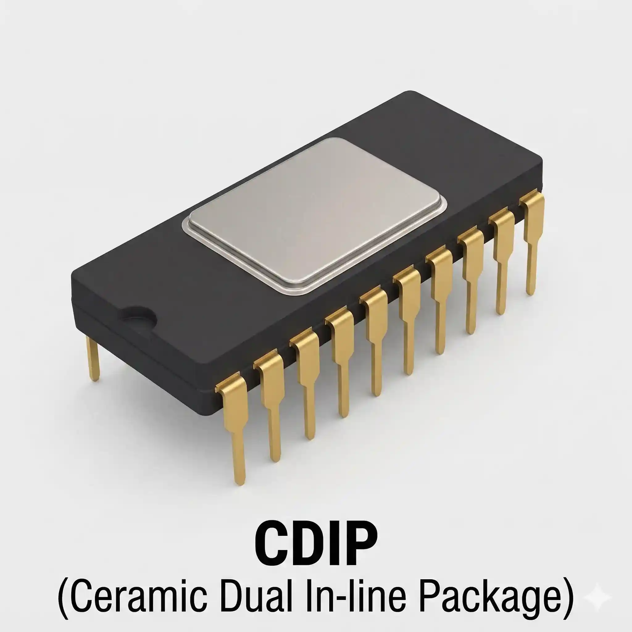
The SNJ54LVC373AJ from Texas Instruments is a military-grade octal transparent D-type latch with 3-state outputs, engineered to provide data buffering and temporary storage in high-reliability digital systems. Housed in a ceramic dual-in-line package (CDIP), this device operates from a 2.7 V to 3.6 V supply and features 5 V tolerant inputs, enabling direct interfacing with legacy 5 V logic in mixed-voltage environments. The eight latches follow the data inputs while the latch-enable (LE) is high and hold the last state on the falling edge of LE; a dedicated output-enable (OE) forces all outputs into a high-impedance state, supporting bus-structured architectures. Characteristic of the LVC family, the latch delivers fast propagation delays and very low static power dissipation, while its full military temperature range of –55°C to +125°C and hermetic ceramic package assure stable operation under thermal and mechanical stress.
Typical deployments span mission-critical aerospace, defense, and rugged industrial platforms, where the latch serves as an address or data buffer in microprocessor modules, bus extenders, and memory-interface circuits that require deterministic signal hold and release. The 3-state outputs permit multiple sources to share common bus lines without contention, a necessity in modular avionics and fail-safe control systems. From a procurement standpoint, the SNJ54 prefix identifies a component manufactured and screened to conformance with military performance standards, delivering documented traceability and extended supply continuity appropriate for high-reliability programs. Nevertheless, military-grade CMOS logic often carries long lead times and may face lifecycle transitions; design and supply-chain teams should verify the active status, source exclusively through authorized channels to guard against counterfeits, and evaluate lifetime-buy strategies when integrating the device into sustainment or new long-life defense designs.
| Attribute | Value |
|---|---|
| Packaging | Tube |
| Standard Pack Qty | 1 |
| Package / Case | J (CDIP), 20 pins |
| Absolute Maximum Supply Voltage | -0.5 V to 6.5 V |
| High-level Input Voltage (VIH) | 2 V (MIN) @ VCC = 2.7 V to 3.6 V |
| High-level Output Current (IOH) | -12 mA @ VCC = 2.7 V |
| Input Voltage (VI) | 0 V to 5.5 V |
| Low-level Input Voltage (VIL) | 0.8 V (MAX) @ VCC = 2.7 V to 3.6 V |
| Low-level Output Current (IOL) | 12 mA @ VCC = 2.7 V |
| Output Voltage (VO) | 0 V to VCC |
| Supply Voltage (Recommended) | 2 V to 3.6 V |
| Operating Temperature | -55°C to 125°C |
| Base Device | SN54LVC373A |
Download the current available datasheet for SNJ54LVC373AJ.
Download Datasheet